INDIA —A major long-term expansion program is slated for India's semiconductor supply chain following a strategic investment commitment by Applied Materials in Karnataka. The US-headquartered semiconductor equipment giant has finalized an agreement to deploy INR 36 billion over a 10-year period to establish advanced research, software development, and equipment manufacturing facilities at the Bengaluru Signature Business Park. This multi-year venture represents the foundational industrial development for the newly planned business district and is projected to generate roughly 1,000 high-skilled technical jobs in the region.
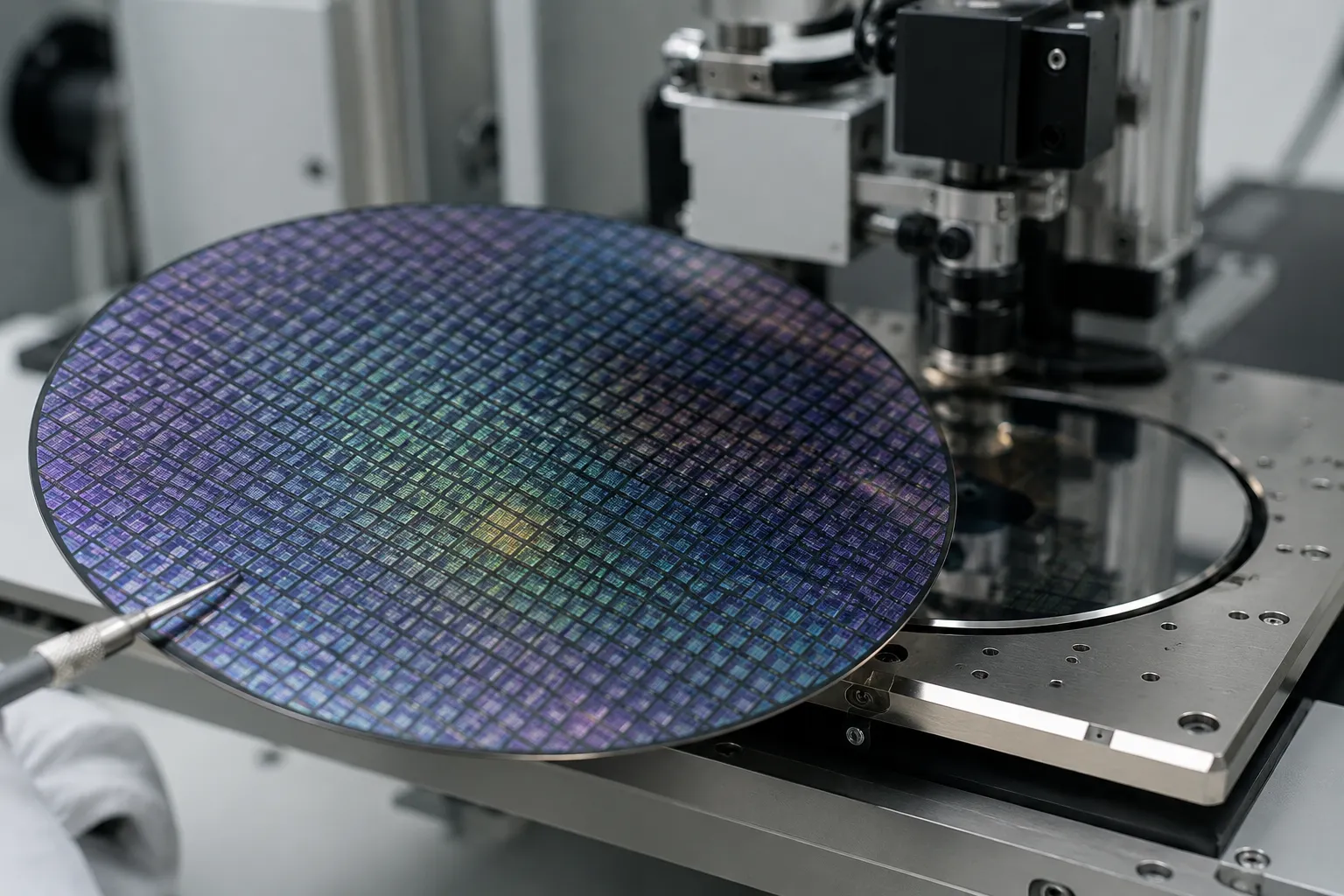
Applied Materials is a global supplier of equipment, software, and materials engineering solutions used to produce semiconductor chips and advanced displays. Operating in India for more than two decades, the corporation recently expanded its operational footprint by opening an 800,000-square-foot campus in Bengaluru, featuring product design, simulation, and 300mm wafer validation capabilities, alongside an artificial intelligence center in Chennai.
This capital deployment addresses crucial gaps in India's technology ecosystem by moving beyond chip design into core hardware manufacturing and process engineering. Upstream equipment design and component testing are essential components for building sub-surface technology infrastructure, allowing local markets to reduce reliance on external suppliers for critical fabrication components.
The arrival of dedicated manufacturing and software units accelerates Karnataka's transition into a high-tech industrial corridor. Regional technology clusters benefit from localized supply networks, reduced component lead times, and enhanced collaboration between international equipment creators and domestic engineering talent. The sustained capital infusion also bolsters government initiatives aimed at attracting high-value capital goods production to the state.
For global chipmakers and equipment vendors, establishing key engineering bases in India provides structural cost advantages and deep talent access. Institutional investors and supply chain vendors are likely to view this expansion as a catalytic anchor project, expected to spur complementary investments in local precision component fabrication, technical training, and software services dedicated to global wafer processing platforms.