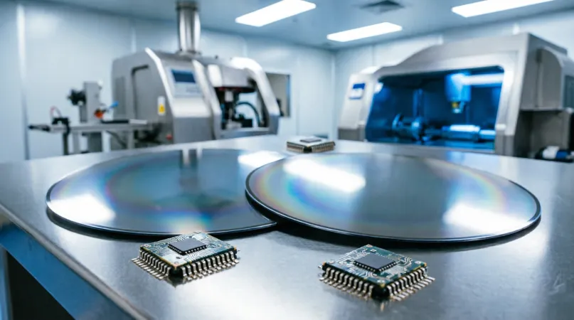
INDIA —Global technology services provider HCLTech has commissioned a state-of-the-art semiconductor engineering and testing center in Bengaluru, India, backed by an investment of Rs 1.85 billion. Spanning 40,000 square feet, the new site features specialized Class 10K and Class 1K cleanroom environments designed to offer comprehensive post-silicon engineering, hardware validation, automated testing, and failure analysis. Operating under the company's Spec2Parts execution framework, the integrated platform unifies early-stage research with production qualification to streamline chip commercialization for global clientele.
This capital expansion addresses critical infrastructure gaps in India's technology ecosystem by consolidating advanced test, probe, and diagnostic tools under one roof. Equipped with advanced automated test equipment, electron microscopy, and focused ion beam systems from leading global measurement vendors, the facility allows semiconductor design firms to reduce turnaround times and minimize supply chain fragmentation. The unit is pursuing aerospace, medical, and industrial quality accreditations to serve both domestic enterprise requirements and international markets.
The investment reflects a strategic shift among technology outsourcing providers toward high-margin, specialized R&D services amid growing global demand for custom silicon, artificial intelligence hardware, and advanced packaging solutions. By establishing localized testing infrastructure, the facility strengthens regional engineering execution while positioning India as an emerging destination for high-end semiconductor R&D and post-design validation.
Headquartered in India, HCLTech is a multinational information technology services and consulting enterprise operating across sixty countries with a workforce exceeding 223,000 employees. The company provides engineering R&D, digital transformation, cloud computing, and enterprise software services to global clients across diverse industry verticals.