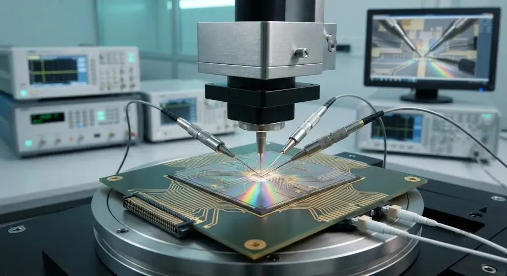
INDIA —India’s Ministry of Electronics and Information Technology has sanctioned Phase II of the Centre for Programmable Photonic Integrated Circuits and Systems initiative, committing an overall project budget of INR 999.4 million. The five-year venture, dubbed SPECTRA, is executed under a Memorandum of Understanding signed between the Indian Institute of Technology Madras and semiconductor manufacturing firm izmo Microsystems. Funding comprises INR 975.4 million from government grant allocation and INR 24 million via cash and in-kind contributions from izmo Microsystems.
Bengaluru-headquartered izmo Microsystems operates as a specialized subsidiary of public entity izmo Limited, delivering semiconductor packaging, testing, and system-in-package architectures across radio frequency, microwave, and silicon photonics sectors. The strategic MoU builds upon Phase I outcomes, shifting focus from initial conceptual research toward commercial-grade design rules, volume packaging, and industrialization. Under this roadmap, primary technical milestones involve engineering a 1.6 Tbps silicon photonics transceiver engine operating at 1550 nm, microwave photonic chips reaching frequencies above 50 GHz, integrated quantum communication systems, and dedicated photonic processors tailored for artificial intelligence workloads. A standardized Process Design Kit housing over 100 IP blocks for 200 mm wafer platforms will also be established.
The expansion comes as global data center architectures encounter physical and thermal limitations driven by intensive high-performance computing demand. Traditional electronic interconnects struggle to maintain efficiency under massive data throughput, elevating optical networking into critical infrastructure. According to market research estimates from LightCounting, global optical transceiver sales reached USD 26.8 billion in 2025 and are projected to hit USD 40 billion in 2026, with silicon photonics accounting for over half the total share. Furthermore, the market for underlying optical chips across transceivers and co-packaged devices is anticipated to expand from USD 4 billion in 2025 to USD 15 billion by 2031.
By directly targeting packaging assembly, high-precision fiber alignment, electronic-photonic co-integration, and thermal validation, the bilateral agreement establishes localized capabilities within India's broader technology self-reliance framework. This operational ecosystem bridges advanced academic chip prototyping with scalable manufacturing, allowing domestic and global supply chain participants in telecommunications, defense, and cloud computing to deploy high-density, low-latency co-packaged optics solutions.