
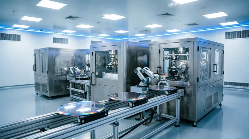
The Indian government has approved the Semicon 2.0 initiative with an allocation of INR 1275 billion to scale up domestic chip design, component fabrication, and precision equipment manufacturing, cementing its role in the global electronics value chain.
The Indian government has approved a major policy update to bolster its domestic electronics value chain, greenlighting the next iteration of its semiconductor support strategy with an allocated capital expenditure of INR 1275 billion. According to official disclosures, the newly sanctioned Semicon 2.0 framework expands upon initial foundational progress to establish a comprehensive manufacturing and intellectual property hub. The central administration aims to deepen its domestic capability by scaling existing operations and bringing advanced technological capabilities into the country over the coming years.
The strategic rollout of this upgraded policy demonstrates India's long-term commitment to overcoming global supply bottlenecks and securing high-value technological sovereign assets. Under the initial phase of the semiconductor initiative, twelve manufacturing operations received formal backing, representing a joint investment commitments surpassing INR 1640 billion. Early commercial production has already commenced from specialized packaging facilities operated by providers such as Micron, Kaynes, and CG Semi, signaling the transition from policy frameworks to viable industrial output. The incoming capital tranche under the revised initiative is designed to address broader upstream bottlenecks, including specialized machinery production and essential raw material chemical processing, while expanding specialized talent pipelines across hundreds of domestic universities.
For global electronics manufacturers and enterprise buyers, this programmatic expansion targets multiple layers of the industrial architecture, spanning advanced silicon fabrication, assembly, testing, and outsourced semiconductor assembly and test operations. Beyond scaling assembly plants, the multi-pillared program channels intensive incentives into complex microchip design startups and mid-tier firms that are currently prototyping system-on-chip architectures for specialized sectors like aerospace, automotive electronics, and artificial intelligence infrastructure. By subsidizing precision engineering equipment and the localized sourcing of high-purity chemicals and gases, the policy creates structural entry points for international chemical majors and toolmakers eyeing partnerships in the South Asian corridor.
From an investment and asset management perspective, the long-term fiscal commitment offers substantial market visibility for multinational corporations seeking geographical diversification outside traditional East Asian fabrication strongholds. With a major commercial fabrication plant scheduled to begin operations by 2028, the secondary ecosystem phase creates extensive opportunities for supply chain integration across consumer appliances, telecom hardware, and smart energy grids. Enterprises looking to mitigate systemic geopolitical risks can leverage these state-backed capital subsidies to establish parallel design clusters and advanced packaging nodes, leveraging an increasingly specialized regional talent pool trained in modern electronic design automation software tools.
About GlobeNewsInfo
GlobeNewsInfo.com is a business news platform providing latest updates on global business developments, projects, and contract opportunities across diverse sectors and regions. The platform is designed to serve as a trusted source of information for companies, investors, and professionals worldwide.