
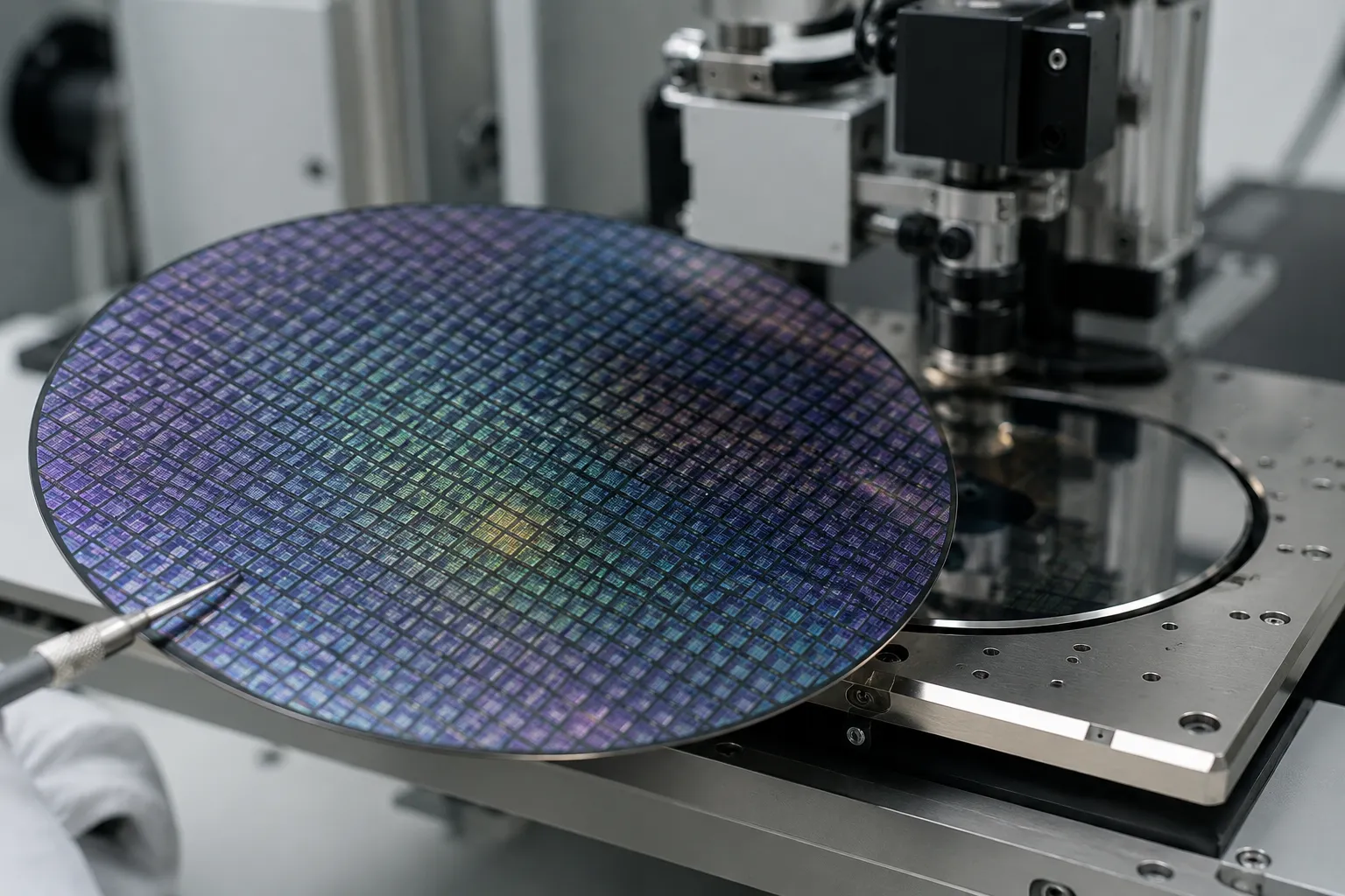
Sony Group and Taiwan Semiconductor Manufacturing Co. are negotiating a joint investment of approximately JPY 1 trillion to build a specialized chip fabrication plant in Japan. Targeted for a 2029 operational launch, the facility will produce next-generation image sensors for automotive and robotic applications.
Sony Semiconductor Solutions and Taiwan Semiconductor Manufacturing Co. are in advanced discussions to allocate a combined JPY 1 trillion toward a joint semiconductor manufacturing facility in Japan's Kumamoto Prefecture. Under the proposed structure, the Tokyo-headquartered consumer electronics and entertainment conglomerate Sony Group will maintain a controlling stake in the venture, while contract chipmaker TSMC will serve as the primary technology partner. Operational output at the new site is targeted to begin in 2029, as reported by international media.
Sony Group Corporation is a global technology and entertainment conglomerate that develops electronics, image sensors, gaming hardware, and media assets. Taiwan Semiconductor Manufacturing Company Limited is the world's largest dedicated contract semiconductor foundry, providing chip fabrication services to leading technology companies globally. The joint project builds on existing infrastructure in Kumamoto, where TSMC already operates advanced fabrication facilities and where both entities maintain existing operational partnerships.
This initiative underscores a strategic pivot for Sony toward industrial automation and autonomous transportation, expanding beyond its traditional consumer mobile sensor client base. The facility will specifically target the fabrication of next-generation optical and image sensors designed for artificial intelligence applications, autonomous vehicles, and industrial robotics. For Japan, the expansion reinforces national policy objectives to rebuild domestic advanced chip production capabilities through strategic public-private partnerships and foreign foundry collaborations.
From a capital allocation perspective, the joint venture allows Sony to pursue a capital-efficient operational model by sharing massive fabrication costs while securing specialized production capacity. The development benefits automotive original equipment manufacturers and robotics developers seeking robust supply chains for advanced sensing hardware. Furthermore, potential subsidies from the Japanese government could reduce capital risk for both partners, accelerating long-term hardware supply resilience across East Asia's technology sector.
About GlobeNewsInfo
GlobeNewsInfo.com is a business news platform providing latest updates on global business developments, projects, and contract opportunities across diverse sectors and regions. The platform is designed to serve as a trusted source of information for companies, investors, and professionals worldwide.